The mosfet has the gate insulated from the substrate by a thin layer of silicon oxide, to prevent gate current flowing and damaging the device (see the page on fets).
There are two main families.
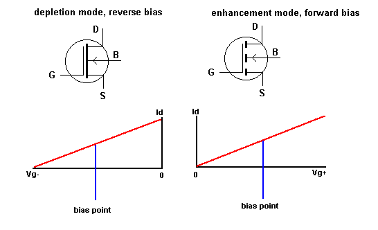
Enhancement - where the mosfet has to be forward biased like a transistor.
Depletion - where the mosfet is reverse biased like a thermionic valve (tube in the USA).
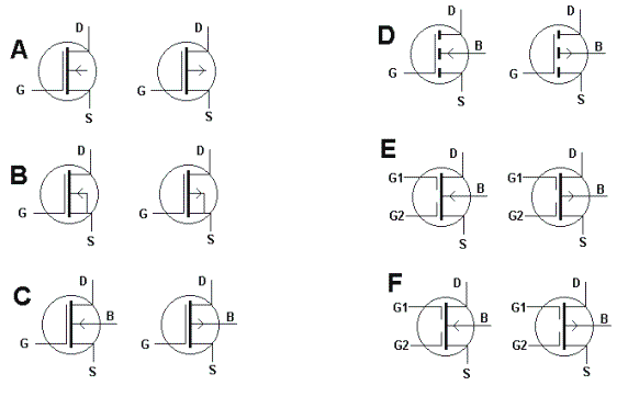
Some mosfets have two gates (dual gate mosfets) and are commonly used as r.f. mixers.
The insulating layer is extremely thin and can be easily damaged by static. Antistatic precautions must be taken when handling them. Soldering iron tips must be earthed. The operator must be grounded via a high value resistor, with wrist straps etc. The workplace must be grounded safely. Components must be handled with care. The operator should touch some earthed point just before handling static sensitive devices.
Some devices have Zener diodes built in, between gate and source, for protection.
The thick line represents the channel and if it is unbroken represents a depletion ( normally conducting) type. If the channel is shown broken it is a normally enhancement (non conducting) type.
|
|